Sunday, January 29, 2017
What is 555 Timer How it Works
What is 555 Timer How it Works
555 Timer
Timers
Timers are those circuits, which provide periodic signals to a digital system which change the state of that system. In other words, those circuits, which work on the base of multivibrator changes or a device, which can be used as multivibrator is called Timer. (We will discuss Multivibrator in detail in next coming posts)
555 Timer
555 Timer is a digital monolithic integrated circuit which may be used as a clock generator. In other words, 555 Timer is a circuit which may be connected as a stable or monostable multivibrator.
555 Timer is a versatile and most usable device in the electronics circuits and designs which work for both stable and monostable states. It may provide time delay from microseconds up to many hours.
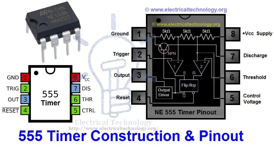
Below is the pin diagram of DIP (Dual inline Package) 555 timer with 8 pins.

555 timer is a very cheap IC which works for wide range of potential difference (typically, from 4.5 to 15V DC) and the different provided input voltages do not affect the timer output.
555 Timer is a linear device and it can be directly connected to the CMOS or TTL (Transistor – Transistor Logic) digital circuits due to its compatibility but, interfacing is must to use 555 timer with other digital circuits.
555 Timer Construction
There are lots of manufacturers who manufacture 555 timer which included the number 555 e.g. NE555, CA555, SE555, MC14 555 etc. typically, two 555 timers sandwiched inside a single chip which is called 556. Nowadays, chips are available with four 555 timers in it. These devices are available in circular IC with eight (8), DIP (Dual inline Package) with 8 pins or DIP with 14 pins.
Here is the simple explanation of the 8 pins of 555 Timer.
1. Ground (GND)
It’s the common ground point of the circuit. The ground terminal of external circuit as well as power supply (Vcc) ground terminal is connected with this i.e. GND (Ground) terminal of 555 timer.
2. Trigger
When Trigger terminal gets one –third (1/3) of the supply voltage i.e. Vcc/3 equal amplitude’s negative trigger pulse, then the circuit output changes form Low to High.
3. Output
This terminal is used for getting output and connected with load. At any instant, its value is low or high.
4. Reset
Without taking into account the previous state of output, by providing a trigger pulse to this terminal resets the device. I.e. Its output becomes low.
5. Control Voltage
There are two third positive voltages of the total Supply voltages (Vcc) at control voltage terminal. Thus, it becomes a part of the comparator circuit. Generally, a capacitor is connected between ground and voltage control terminals.
6. Threshold Voltage
Threshold voltage and control voltage is the two inputs of comparator circuit. The circuit compares the available voltage at threshold voltage terminal to the available reference voltage at control terminal.
If the available voltage at threshold terminal (Pin 6) is greater than the control voltage i.e. two-third of Vcc, then the output would be low, otherwise, it would be high.
7. Discharge
When output is low, then Discharge terminal provides a low resistance discharge path to the externally connected capacitor. However, it acts an open circuit, when output is high.
8. +Vcc (Supply Voltage Terminal)
Supply voltage is provided at this terminal for timer operation.
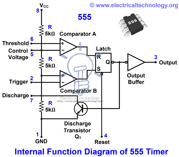
A simple 555 timer circuit is shown below in fig _ which shows the internal construction of 555 timer. According to the fig, the timer contains on two comparators, an RS flip flop, an Output stitch (output buffer) and a Discharge Transistor Q1.
In addition, there are three 5k? resistors are connected in series with 5k? resistor which first end is connected with Vcc (Pin 8 = Supply voltage) and the other end is connected with ground (GND = Pin 1).
Good to Know: due to the three 5k? series connected resistors, this IC timer chip is called 555 Timer J.
Working Principle of 555 Timer

In the 555 Timer block or functional diagram, comparators are those devices which output is high, when their positive input voltage is greater than their negative input voltage and vise versa.
The voltage divider in the circuit (which contains on three series connected 5k? resistors), which provides the trigger level of one-third of Vcc (Vcc/3) and two-third (2/3) of threshold voltage. To understand this point, suppose the input value is 15V. In this case, the value of trigger level would be 5V as (Vcc/3 = 15V/3 = 5V). And the value of threshold level would be 10V as (Vcc x 2/3 = 15V x (2/3)) = 10V.
When needed, the trigger level and threshold can be adjusted by using the Control Voltage terminal (Pin 5) i.e. by changing the control voltage at Pin 5, we may change the trigger level and threshold voltage according to the required specification. However, in this case, the value of trigger and threshold would be remain equal to 1/3 Vcc and 2/3 Vcc respectively.
When the normal high trigger input value instantaneously reduce then the 1/3 Vcc, Then the output of Comparator B becomes High from Low, as a result, RS latch or RS Flip flop goes to “set”. When flip flop goes to set, then Output (at Point 3) becomes high. Simultaneously, the discharge transistor Q1 gets off and The output remains high until the value of normally low threshold input does not increase then the 2/3 Vcc.
As soon as the threshold input increase than the 2/3Vcc, then the output of comparator A becomes Low, as a result, RS flip flop get reset (because the output of comparator is directly connected to the RS flip flop’s input R as shown in the fig). When flip flop gets reset, output becomes low and discharge transistor Q1 goes to on.
The flip flop can be reset by applying external input reset without threshold circuit. Note that, the trigger and threshold inputs (Pin 2 and Pin 6) are controlled by externally components and the 555 timer can be used for Available link for download